
The design of modern integrated circuits has shifted from simple logic implementation to complex System-on-Chip (SoC) architectures that balance computational density, thermal envelopes, and manufacturing yield. As feature sizes approach the atomic scale, the margin for error in physical design diminishes, forcing architects to reconcile the abstract logic of software with the unforgiving realities of silicon physics.
Understanding modern chip [architecture](/blog/postgresql-vs-mysql-the-storage-decision-that-can-make-or-break-your-architecture) requires looking beyond the instruction set architecture (ISA). It demands a holistic view of data movement, power distribution, and the limitations imposed by lithographic resolution. Engineering at this scale is an exercise in managing trade-offs between latency, throughput, and power dissipation.
Architectural Paradigms: The SoC Shift
The transition toward SoC architectures was driven by the need to minimize inter-chip communication latency. By integrating memory controllers, specialized accelerators, and I/O interfaces onto a single die, architects significantly reduced the power overhead associated with off-chip signaling. However, this integration complicates thermal management, as concentrated power density can create hotspots that degrade transistor switching characteristics.
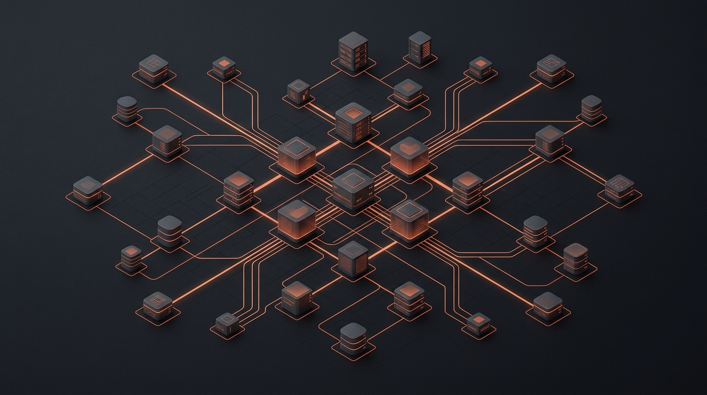
Modern SoCs rely heavily on Network-on-Chip (NoC) topologies to manage communication between heterogeneous cores. Unlike traditional bus-based architectures, a NoC uses packet-switched routing, allowing for concurrent data flows and improved scalability. This shift introduces non-deterministic latency, which must be accounted for in the firmware and OS scheduler design.
Balancing Heterogeneous Compute
The inclusion of specialized accelerators—such as NPUs for tensor operations or ISPs for image processing—is now standard. These units offer orders-of-magnitude better performance-per-watt than general-purpose CPUs. The architectural challenge lies in the memory hierarchy; these accelerators often require high-bandwidth memory (HBM) or large scratchpad caches to prevent the CPU from becoming a bottleneck during data orchestration.
The Manufacturing Lifecycle and Yield Engineering
Semiconductor manufacturing is an iterative process defined by Design for Manufacturing (DFM) rules. As nodes shrink to 5nm and below, techniques like Multi-Patterning and Extreme Ultraviolet (EUV) lithography become mandatory. These technologies ensure that the physical layout matches the intended logical design, despite the diffraction limits of light.
The primary objective of DFM is to maximize yield by ensuring that critical paths are robust against the process variations inherent in etching and deposition.
Yield is the percentage of functional chips on a wafer. It is highly sensitive to defect density and die size. Larger dies are inherently more susceptible to random defects, leading to an exponential drop in yield. This is why architects often prefer ‘chiplet’ designs, where a large SoC is broken into smaller, independently manufactured components connected via high-speed packaging technologies.
Performance Bottlenecks and Thermal Constraints
Performance in modern circuits is rarely limited by raw switching speed; it is limited by data movement. The ‘memory wall’ remains the most significant hurdle. Even with fast caches, the energy cost of moving data from DRAM to the execution units often dwarfs the energy cost of the computation itself.
// A simplified model of power consumption in a logic gate
// P_total = P_switching + P_leakage + P_short_circuit

float calculate_gate_power(float frequency, float capacitance, float voltage) {
    float p_switching = 0.5f * capacitance * (voltage * voltage) * frequency;
    // Leakage increases exponentially with temperature and process node shrinking
    float p_leakage = calculate_leakage(voltage, temperature);
    return p_switching + p_leakage;
}
Thermal management is not merely a cooling issue; it is a fundamental design constraint. High temperatures increase leakage current, which in turn increases power consumption, creating a positive feedback loop that can lead to thermal runaway. Architects use dynamic voltage and frequency scaling (DVFS) to keep the chip within its Thermal Design Power (TDP) limits, often sacrificing peak performance to maintain long-term stability.
Future Directions in Circuit Design
- 3D Stacking: Moving beyond 2D planar layouts to vertical integration to reduce interconnect length.
- Optical Interconnects: Replacing copper traces with on-chip photonics to overcome electrical signal degradation.
- Near-Threshold Computing: Operating at voltages near the transistor threshold to achieve extreme energy efficiency at lower clock speeds.
Conclusion
The evolution of circuit architecture is increasingly defined by the integration of hardware and software co-design. As we push the limits of classical silicon, the focus shifts toward more efficient data movement, novel packaging, and specialized acceleration. Successful system design in this domain requires a deep appreciation for both the abstract logic of high-level code and the concrete physical constraints of the silicon it inhabits.